Jablonski Diagram – important discovery in OLED chemistry
Noctiluca is the Polish company with DNA based on science. Torun, our hometown, is the birthplace of astronomer Nicolaus Copernicus, the patron of the largest institution of higher education in the city – the Nicolaus Copernicus University. It is in the premises of this university that our laboratory operates. And it is with this university that a famous Polish scientist was associated. In 1946 Aleksander Jablonski, the author of the Jablonski Diagram, settled in Toruń where he was appointed Head of the Faculty of Physics at the NCU. His work is still relevant today in such modern areas as the display industry.
The Jablonski Diagram, conceptualized in 1933, is more than a schematic—it’s a comprehensive framework for visualizing molecular behavior under photo-excitation. This diagram is invaluable for OLED material manufacturers as it intricately maps the energy levels of molecules, both electronic and vibrational, in response to light. It’s particularly insightful in demonstrating how these energy levels are schematically represented and how they increase along the vertical axis, illustrating the nuanced energy states and transitions important for OLED technology.
Jablonski Diagram: fundamentals and significance of electronic processes
The diagram’s depiction of various electronic states—singlet and triplet (S0, S1, T1, etc.)—and their vibrational counterparts is pivotal for understanding OLED material behavior. By illustrating the transitions between these states, both radiative and non-radiative, the Jablonski Diagram offers a deeper comprehension of the photophysical phenomena in OLED components. It shows how these transitions occur through straight and curved lines, representing interactions with and without light, respectively. This aspect is crucial for OLED material manufacturers, as it enables the prediction and manipulation of luminescent behaviors in OLED materials.
Evolution and applications of the Jablonski Diagram in modern OLED technology
As OLED technology has advanced, so has the Jablonski Diagram, evolving to illustrate the increasing complexity of OLED materials. It now represents a more intricate overlap of vibronic and electronic energy levels, reflecting the complex behavior of modern OLED materials. This detailed representation aids OLED material manufacturers in developing new materials and enhancing the operational efficiencies of OLED devices, particularly in high-efficiency lighting and high-quality display screens.
Process analysis: absorption, excitation, and vibrational relaxation in the context of the Jablonski Diagram
The diagram excellently visualizes the absorption of a photon by a molecule, a rapid process leading to the molecule’s transition from its ground state (S0) to an excited singlet or triplet states (like S1 or T1). This process is swiftly followed by vibrational relaxation, depicted as a curved arrow in the diagram. This stage, where excess vibrational energy is dissipated, typically as heat, is essential for understanding the efficiency and stability of OLED materials, as it leads the molecule to the lowest vibrational level of the excited state.
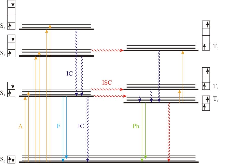
Modified Jablonski diagram of energy transitions. Wavy arrows indicate transitions – non-radiative,
straight arrows – radiant, A – absorption, F – fluorescence, Ph – phosphorescence, IC – internal conversion,
ISC – intercombination transition.
TADF emitters in the Jablonski Diagram: phenomena in OLED chemistry
Jablonski diagram is an important tools in understanding the photophysical processes involved in Thermally Activated Delayed Fluorescence (TADF) emitters. It illustrates the energy levels and transitions that occur within a molecule upon absorption of light. For TADF emitters, Jablonski diagram explains the pathways through which non-radiative processes are suppressed, allowing delayed fluorescence to occur, which is crucial for improving the efficiency of organic light-emitting diodes (OLEDs). By providing a clear visual representation of these energy transfer mechanisms, Jablonski diagram enables researchers in the design and optimization of TADF emitters for various optoelectronic applications.
Practical applications of the Jablonski Diagram in OLED material development
- Material synthesis and design: The Jablonski Diagram plays a critical role in the synthesis and design of OLED materials. OLED material designers/chemists leverage the diagram to predict how new organic compounds behave under different lighting conditions. This predictive capability is essential for designing materials that not only exhibit specific luminescent properties but also align with the stringent requirements of OLED displays and lighting systems. By understanding the electronic and vibrational transitions depicted in the diagram, researchers can innovate materials that offer better performance and unique characteristics suited for diverse applications.
- Efficiency optimization: One of the key applications of the Jablonski Diagram in OLED technology is in optimizing the efficiency of OLED devices. The diagram helps in identifying and understanding the various pathways of energy loss within OLED materials. By minimizing non-radiative transitions, which are typically represented as curved lines in the diagram, OLED material manufacturers can significantly enhance the luminous efficiency of their products. This optimization is crucial in developing high-performance OLED displays and lighting systems that consume less power and offer brighter output.
- Tailoring color properties: The Jablonski Diagram is instrumental in tailoring the color properties of OLED materials. By manipulating the transitions between different energy states, chemists can precisely control the emission spectrum of OLED materials. This control is pivotal for producing color-specific diodes, a critical aspect of high-quality display screens. The ability to fine-tune these transitions allows deeper color saturation, making OLED technology the preferred choice for high-end display applications.
- Lifetime and stability improvement: Improving the lifetime and stability of OLED materials is another crucial application of the Jablonski Diagram. Insights gained from the diagram guide researchers in reducing degradation pathways, such as triplet-triplet annihilation or photo-oxidation. By understanding how different electronic states interact and lead to material degradation, chemists can develop OLED materials that are more stable and have longer operational lifetimes. This improvement is vital for ensuring the long-term reliability and performance of OLED-based products.
- Advanced applications and innovations: The Jablonski Diagram continues to inspire innovations in OLED technology. Advanced applications, such as flexible or transparent OLED displays, are being explored thanks to the deeper understanding of molecular transitions provided by the diagram. This knowledge is driving the development of next-generation OLED materials that could revolutionize the way we interact with displays and lighting systems. The potential for creating thinner, more energy-efficient, and environmentally friendly OLEDs is a direct consequence of the insights provided by the Jablonski Diagram.
The impact of the Jablonski Diagram on emerging OLED technologies
- New OLED applications: The Jablonski Diagram is not just used in OLED technologies but is also paving the way for new applications, beyond traditional displays and lighting. This includes flexible electronics, where OLEDs can be integrated into wearable devices.
- OLEDs in sustainable and eco-friendly technologies: The Jablonski Diagram is also instrumental in driving OLED technologies towards more sustainable and environmentally friendly solutions. By understanding the photophysical processes, researchers are developing OLED materials that are more efficient, have a longer lifespan, and use less harmful substances. This shift is crucial in reducing the environmental impact of display and lighting technologies.
- Next-generation photonic devices: the Jablonski Diagram is central to the development of next-generation photonic devices. This includes OLEDs with tunable properties for advanced communication systems and photonics-based computing. The diagram’s insights into energy states and transitions are key in developing materials that can function in these applications.
- OLEDs in smart windows and architecture: emerging applications of OLEDs in smart windows and architectural designs are also benefiting from the insights provided by the Jablonski Diagram. These applications require OLED materials that can adapt to different lighting conditions and offer transparency when needed. The diagram assists in designing materials that meet these unique requirements, enabling OLED technology to integrate seamlessly into smart buildings and futuristic architecture.
The Jablonski Diagram remains an indispensable tool in OLED science. Its detailed and accurate representation of photophysical processes is invaluable for OLED material suppliers and researchers. As OLED technology progresses, the principles depicted in this diagram will continue to be significant in driving advancements in this field.
Peter Wiliam Atkins: Chemia fizyczna. Wydawnictwo Naukowe PWN, 2001, s. 489–490. ISBN 978-83-01-13502-7.
Józef Szudy, Andrzej Bielski: Aleksander Jabłoński (1898–1980). Fizyk, muzyk, żołnierz. Toruń: 2010. ISBN 978-83-231-2551-8